0%

As the demand for wafer production ramps up, semiconductor buyers are taking a close look at ceramic chucks — it's no surprise, given how crucial they are. According to WSTS’s Autumn 2024 forecast, worldwide semiconductor sales are expected to hit around $697 billion in 2025, which is roughly an 11.2% jump from before. Meanwhile, SEMI’s World Fab Forecast keeps tabs on ongoing investments in manufacturing capacity, painting a pretty clear picture of a growing equipment market. But honestly, all these reports don’t necessarily mean that every type of chuck will see the same level of demand — it varies depending on specific needs.

When it comes to ceramic chucks, there’s a lot to consider. Whether you need an electrostatic chuck, a vacuum one, or a porous ceramic design, each has its own way of supporting and holding onto wafers. Materials like alumina and aluminum nitride are pretty common choices, but factors like operating temperature, wafer size, flatness, and compatibility with your process really influence what you pick. In reality, a chuck that works great on one piece of equipment might not be the best fit for another — details really do matter here.

This guide breaks down the main ceramic chuck types you’ll want to know about for 2026. It covers typical uses, the pros and cons, and some key questions to ask suppliers about surface quality, how they handle heat, cleaning processes, and how long they tend to last. Even small differences can make a big impact, so it’s not just about specs — you gotta look at actual process data and do some testing on your own equipment. Claims from suppliers are helpful, but making sure they line up with your recipes and maintenance history is the real deal. And yeah, terminology can sometimes be a bit confusing, but that’s just part of the game when you’re sourcing this stuff. So, it’s good to be aware of these quirks and take everything with a grain of salt.

2026 Top Ceramic Chuck Types for Semiconductor Buyers

Define Ceramic Chuck Types by Holding Force: Vacuum, ESC, and Hybrid

2026 Top Ceramic Chuck Types for Semiconductor Buyers

Define Ceramic Chuck Types by Holding Force: Vacuum, ESC, and Hybrid

Choosing a ceramic chuck starts with how it holds the wafer. SEMI’s 2024 300mm Fab Outlook projects global capacity approaching 10 million wafers per month by 2027. That growth raises the value of stable, repeatable wafer handling. It does not make one chuck type right for every process.

Vacuum chucks use pressure differential through ports or grooves. They suit wafers with a sufficiently flat, sealed backside. A small leak can weaken the hold. Dust and surface variation matter.

Electrostatic chucks, or ESCs, attract wafers using voltage across a dielectric. They can clamp without vacuum grooves and support close thermal contact. But voltage, dielectric condition, and residual charge affect release. Not always simple.

Hybrid chucks combine vacuum and electrostatic holding. They can help when wafer conditions or process steps vary, but their control and qualification are more involved.

Holding force alone is an incomplete buying metric. Check wafer bow, backside condition, temperature range, release time, and particle sensitivity under actual recipes.

A chuck that grips strongly on a clean test wafer may behave differently after repeated thermal cycles. This is easy to underestimate.

SEMI’s capacity forecast describes industry scale, not chuck performance; buyers still need process-specific testing and documented acceptance criteria.

Explain ESC Physics: Coulomb and Johnsen–Rahbek Clamping Mechanisms

For semiconductor buyers, an electrostatic chuck’s holding mechanism affects wafer stability, heat transfer, and release behavior. SEMI’s June 2024 World Fab Forecast projected global fab-equipment spending at $110 billion in 2024 and $114 billion in 2025. That scale signals continued investment, not proof that any chuck design performs better. Buyers should match the mechanism to process conditions, including temperature, voltage, and backside gas pressure.

With Coulomb clamping, embedded electrodes create an electric field across an insulating ceramic. The field attracts the wafer toward the chuck. Simple model. Johnsen–Rahbek (JR) clamping uses a slightly conductive dielectric, allowing limited charge movement near the wafer interface. This can increase holding force, but release may take longer as residual charge dissipates. Material resistivity, surface contact, and temperature all matter. In practice, the boundary between the two mechanisms is less tidy than diagrams suggest. Ask suppliers for force and dechucking data under your actual process conditions, not voltage ratings alone.

2026 Top Ceramic Chuck Types for Semiconductor Buyers - Explain ESC Physics: Coulomb and Johnsen–Rahbek Clamping Mechanisms

Chuck type Clamping mechanism Common ceramic construction Typical process fit Buyer considerations
Coulomb-mode ESC Electrostatic attraction across the dielectric. In an idealized model, pressure increases with dielectric permittivity and the square of electric field, and decreases with the square of dielectric thickness. Typically a relatively high-resistivity ceramic dielectric, often alumina or aluminum nitride (AlN), over embedded electrodes. Wafer processing where stable holding, controlled wafer temperature, and a defined de-chucking sequence are required. Check dielectric thickness and uniformity, electrode layout, operating voltage, wafer contact, and residual-charge management. Actual force depends on surface condition and the full chuck design.
Johnsen–Rahbek (JR) ESC Uses a controlled voltage drop across the ceramic and microscopic wafer–chuck contact regions. Interfacial polarization can produce stronger attraction than a simple ideal Coulomb model predicts. A ceramic engineered with finite, controlled electrical resistivity; alumina-based formulations are commonly used. Resistivity is design- and temperature-dependent. Applications that benefit from strong clamping, including processes where wafer contact and thermal coupling are important. Evaluate leakage current, temperature sensitivity, contact condition, charge decay, and release behavior. JR performance depends on resistivity, surface finish, and operating conditions.
Bipolar electrode ESC Two electrode poles are driven at opposite potentials. The electric field acts through the dielectric; this is an electrode arrangement and can be implemented with Coulomb or JR behavior. Ceramic dielectric with embedded, electrically isolated electrode patterns; material selection depends on thermal, electrical, and plasma requirements. Common choice for conductive or semiconductive wafers and many plasma process tools. Confirm power-supply compatibility, pole balance, electrode insulation, and de-chuck controls. Bipolar describes the electrode configuration, not a separate clamping-force law.
Monopolar electrode ESC A single driven electrode creates an electric field with the wafer and its electrical path serving as the opposing side of the system. Ceramic dielectric over a single embedded electrode; the exact ceramic and resistivity depend on the intended clamping mode. Selected tools and wafer configurations with a suitable conductive path and established grounding arrangement. Check wafer conductivity, backside condition, grounding, and compatibility with the process chamber. Suitability is more dependent on wafer and tool electrical configuration than with many bipolar designs.
Alumina ceramic ESC Can be designed for Coulomb-mode or JR-mode operation; the ceramic composition and electrical resistivity determine the electrical behavior. Aluminum oxide (Al2O3), selected for electrical insulation, wear resistance, and established ceramic manufacturing processes. A broad range of semiconductor applications; suitability depends on thermal load, plasma exposure, and required electrical properties. Review thermal conductivity, purity, surface finish, dielectric properties, and compatibility with process chemistry. Properties vary by grade and fabrication.
Aluminum nitride (AlN) ceramic ESC Can use Coulomb or JR clamping, depending on electrode design and the electrical properties of the ceramic. Aluminum nitride (AlN), commonly selected where high thermal conductivity is valuable; actual performance depends on grade and construction. Processes with demanding wafer-temperature uniformity or heat-transfer requirements, subject to tool and process compatibility. Assess thermal uniformity, ceramic purity, plasma and chemical compatibility, electrode integration, and total cost. High ceramic thermal conductivity alone does not guarantee uniform wafer temperature.

Note: ESC voltage, clamping force, ceramic resistivity, and release time are design-specific and depend on wafer properties, temperature, surface condition, and process environment. Compare qualified operating data under representative conditions rather than treating any single value as universal.

Compare Monopolar and Bipolar Electrodes for Plasma Wafer Processing

During plasma wafer processing, electrode layout affects how clamping voltage reaches the wafer. A monopolar ceramic chuck uses one embedded electrode, while the wafer and chamber system complete the electrical return path. This design can be straightforward, but its performance may depend more on wafer conductivity, grounding, and plasma conditions. Small details matter.

A bipolar chuck places two electrodes beneath the ceramic surface and applies opposite potentials. This arrangement can provide more independent clamping behavior when plasma conditions change, and may suit wafers that are difficult to clamp with a monopolar design. It also demands careful electrode spacing and insulation. Not automatically better. Electrode geometry, ceramic quality, and voltage settings still shape uniformity and release behavior.

For buyers, compare more than nominal holding force. Review wafer-temperature uniformity, backside-gas sealing, edge stability, and dechucking time under representative process conditions. Ask how performance changes across wafer materials and thicknesses. A neat electrode diagram is not proof of reliable release; test data matters more. I would also inspect results after repeated thermal cycles, because small drift can become visible at the wafer edge. The best choice depends on the chamber, process window, and maintenance priorities.

2026 Top Ceramic Chuck Types for Semiconductor Buyers

Monopolar vs. bipolar electrodes for plasma wafer processing

A monopolar chuck has one driven electrode; a bipolar chuck has two electrodes driven with opposite polarity. This chart compares electrode count only—not clamping force, wafer temperature uniformity, or process performance, which depend on the chuck design and operating conditions.

Compare AlN (170–230 W/m·K) and Alumina (20–30 W/m·K) Ceramics

2026 Top Ceramic Chuck Types for Semiconductor Buyers
Compare AlN (170–230 W/m·K) and Alumina (20–30 W/m·K) Ceramics

Thermal conductivity changes how quickly a ceramic chuck can spread heat from a wafer. Aluminum nitride (AlN), at about 170–230 W/m·K, moves heat substantially faster than alumina, typically around 20–30 W/m·K. These room-temperature ranges reflect values reported in the ASM Handbook, Volume 4A: Ceramics and Glasses, and NISTIR 6853, which evaluates sintered alumina. Actual performance depends on purity, porosity, and manufacturing quality. Numbers alone do not tell the whole story.

For buyers, AlN can help even out temperature across a chuck during demanding thermal processes. Alumina conducts less heat, but may suit applications where its electrical insulation, established processing, or cost profile matters more. Think of a wafer edge warming unevenly: higher conductivity may help move heat across the surface, but chuck design and contact conditions still matter. Not always. A material’s conductivity is not a direct measure of temperature uniformity in a finished assembly. Review data at operating temperature, and ask for lot-specific measurements; a datasheet range can conceal meaningful variation. It is worth checking the measurement method, too. In practice, I would not choose a chuck on conductivity alone.

Match Chuck Diameter to SEMI M1 Wafer Sizes: 150, 200, and 300 mm

SEMI M1 wafer formats commonly used in equipment planning are 150, 200, and 300 mm. Match the chuck to the wafer’s nominal diameter, but do not treat the numbers as the whole specification. A 200 mm wafer needs a chuck engineered for its edge support, hold-down method, and process conditions—not simply a surface labeled “200 mm.”

Check the usable chuck area, wafer pocket or locating features, and edge clearance against the tool drawing. Vacuum zones should hold the wafer securely without interfering with the process area. For a 300 mm wafer, also review flatness, thermal behavior, and compatibility with the handling system. Small mismatches can cause poor seating or uneven contact. That matters.

The nominal diameter is a starting point, not an approval criterion. Confirm the wafer’s edge profile and backside requirements, then compare them with the chuck drawing and operating limits. For 150 mm tools, legacy fixtures may have different locating features than newer designs. Purchase documents can be oddly incomplete here. I would verify the actual wafer-to-chuck interface before ordering, especially when replacing an existing part.

Select by Process Limits: Temperature, Flatness, Helium Pressure, and RF Compatibility

2026 Top Ceramic Chuck Types for Semiconductor Buyers

Ceramic chuck selection starts with the process window, not a material label. Alumina and aluminum nitride differ in thermal behavior, electrical properties, and heat transfer. Those differences matter when wafers face repeated heating and cooling. Check the specified operating range, ramp rate, and temperature uniformity. A room-temperature rating alone can mislead. Small details matter.

Flatness should be reviewed at operating temperature and under the intended wafer load. A chuck that appears flat on a bench may behave differently when warm. Ask for measurement conditions and tolerance data, not just a single headline figure. Backside helium pressure also needs a process-based check. Confirm that seals and gas grooves maintain stable contact across the required pressure range. Leaks or uneven flow can weaken heat transfer.

For RF processes, assess dielectric loss, electrode layout, grounding, and compatibility at the actual frequency. Ceramic composition is only part of the picture. Request test data for the chuck configuration you plan to use, including temperature and pressure limits. I would avoid assuming that a design proven on one tool will transfer unchanged to another. It may, but the interface and operating conditions still deserve review.

Precision Ceramic Chucks for Semiconductor Equipment: Market Insights from SEMI’s World Fab Forecast

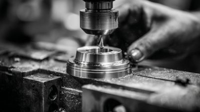
SEMI’s World Fab Forecast projected that global semiconductor fab equipment spending would rise 14% to $109 billion in 2025, reflecting continued investment in production capacity. That expansion places greater emphasis on equipment components that can maintain stable performance through demanding process conditions. Ceramic chucks support wafer handling and positioning, where dimensional accuracy, surface quality, and resistance to heat and corrosive environments are essential. As fabs add and upgrade equipment, durable ceramic parts can help meet the requirements of processes involving high temperatures, vacuum, and corrosive gases.

Manufactured from high-purity alumina powder, these ceramic components are formed by cold isostatic pressing, sintered at high temperature, and precision-finished. They can achieve dimensional tolerances of ±0.001 mm and a surface finish of Ra 0.1, with temperature resistance up to 1600°C. Their wear and corrosion resistance, low thermal expansion, and electrical insulation make them suitable for long-term use in semiconductor production equipment. In this context, precision-machined ceramic chucks offer equipment designers a material option for reliable wafer support as manufacturing capacity grows.

FAQS

How does a vacuum ceramic chuck hold a wafer?

It uses pressure differences through ports or grooves to hold a flat, sealed backside. A small leak can weaken its grip.

When is an electrostatic chuck useful?

It attracts the wafer with voltage across a dielectric, without vacuum grooves. Close thermal contact can help. Release can be tricky.

What makes a hybrid chuck different?

It combines vacuum and electrostatic holding for changing wafer conditions or process steps. More control means more qualification work.

Is stronger holding force always better?

No. Check wafer bow, backside condition, temperature range, release time, and particle sensitivity under real recipes. Test conditions matter.

How do Coulomb and Johnsen–Rahbek clamping differ?

Coulomb clamping uses an insulating ceramic and an electric field. Johnsen–Rahbek clamping uses a slightly conductive dielectric, which can increase force but slow release. Simple models can mislead.

How can residual charge affect wafer release?

Charge may remain after voltage is removed, delaying dechucking. Ask for release data at your process temperature. Not just voltage ratings.

How do monopolar and bipolar electrodes differ?

A monopolar design uses one embedded electrode and relies on the wafer and chamber for the return path. A bipolar design uses two oppositely driven electrodes.

What should buyers test before choosing a chuck?

Compare temperature uniformity, backside-gas sealing, edge stability, and dechucking time with representative wafers. Repeat thermal cycles too; drift may appear near the edge.

Conclusion

Choosing the right Ceramic Chuck Semiconductor solution begins with understanding how each design holds a wafer. Vacuum chucks rely on pressure differential, electrostatic chucks (ESCs) use electrical forces, and hybrid designs combine holding methods. ESCs may operate through Coulomb attraction or the Johnsen–Rahbek effect, while monopolar and bipolar electrode layouts offer different approaches to wafer clamping in plasma processes.

Material and equipment compatibility also shape selection. Aluminum nitride, with thermal conductivity typically around 170–230 W/m·K, supports efficient heat transfer; alumina, at approximately 20–30 W/m·K, may suit applications with different thermal requirements. Match chuck diameter to the 150, 200, or 300 mm wafer sizes associated with SEMI M1, then verify operating temperature, surface flatness, helium pressure needs, and RF compatibility against the process limits.

Benjamin

Benjamin

Benjamin is a dedicated marketing professional at St.Cera Co., Ltd., a renowned private high-tech enterprise specializing in precision ceramic manufacturing. With a deep understanding of the intricacies of ceramic technology, he plays a pivotal role in showcasing the company's innovative products......
Previous Why Choose Ceramic Heater Semiconductor for Global Sourcing?